
Groq3 LPX yield stood at about 33% in April—one working chip for every three on a wafer. By late August it had reportedly crossed 80%, the threshold the industry treats as stable mass production, and Nvidia stood up at Hot Chips 2026 on Stanford's campus to announce the chip was in full production, per Nvidia.
The part that matters for foundry watchers is who built it: Samsung, not TSMC, on the 4nm S5 line at Pyeongtaek—Samsung's only dedicated foundry production line.
That is a genuine milestone. A shipping component inside a shipping Nvidia product, manufactured by the foundry that has trailed on yield for years and lost money doing it.
A shipping component inside a shipping Nvidia product, manufactured by the foundry that has trailed on yield for years and lost money doing it.
Now puncture the triumph. The Groq3 LPX is a 4nm inference accelerator, and Samsung got good at it the way analysts openly say: by making HBM base dies on the same 4nm-class process, where its yields reportedly already run above 90%.
That is not a coincidence—it is the whole point. The base die connects DRAM stacks to the compute device and shuttles data; it is functionally I/O-adjacent work. The process discipline Samsung learned there transferred cleanly to Groq3 because it is the same kind of work.
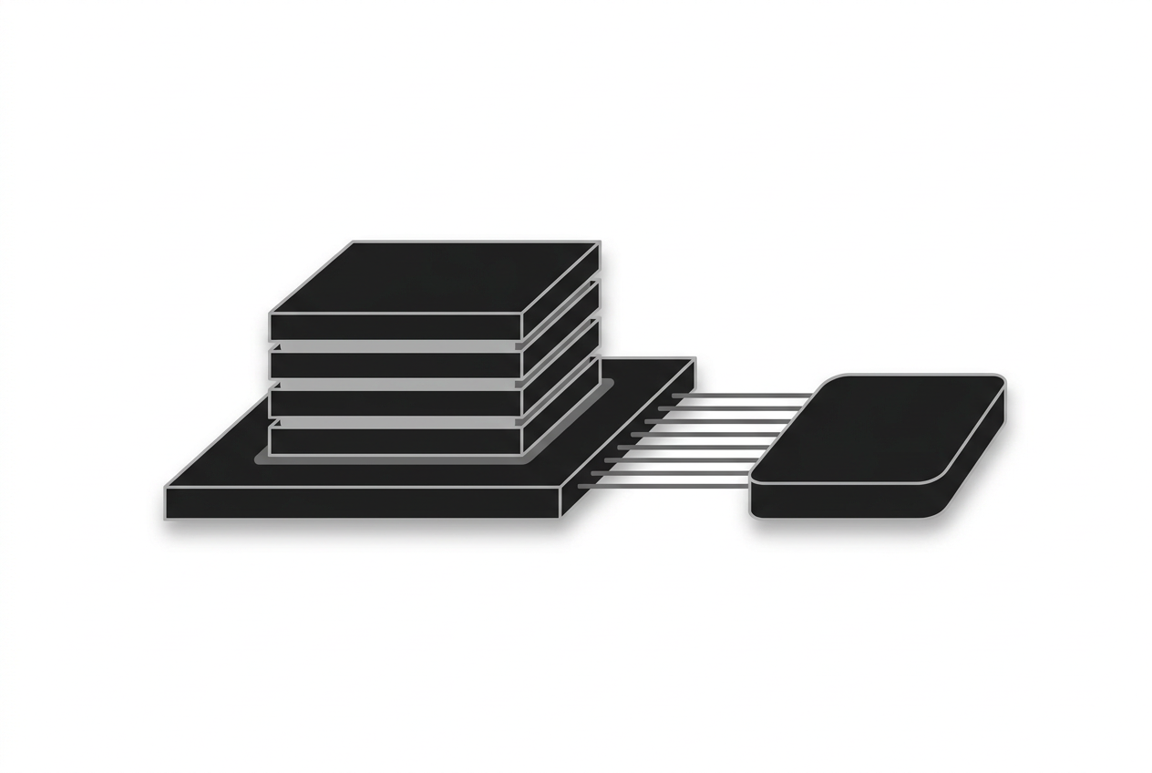
And it is precisely the kind of work that never touched TSMC's leading edge. Nvidia's GPUs—the Vera Rubin parts that fill the rest of Huang's data centers—still come from TSMC. Samsung reportedly got the decode-phase inference chip Huang allocates a quarter of coding-application space to. TSMC kept everything else.
Last week we tracked whether the Intel and Google diversification wins would convert to repeat orders or revert once TSMC's 2028 A14 capacity lands. This week the question sharpens, because two of those bets got concrete: Groq3 is now in mass production at Samsung, and Google's Intel commitment has a number.
The number: Google has reportedly committed to more than 3 million TPUs from Intel for 2028 production, after months of testing Intel's advanced packaging. Google's total TPU output for 2027–2028 is reportedly projected above 6 million units.
Read that commitment carefully. Google tested Intel's packaging—not its logic node—for months before committing. The wedge is EMIB, the embedded silicon bridge that connects processor and memory more cheaply than TSMC's CoWoS.
Nvidia, by contrast, is reportedly still only testing Intel's process for its 2028 Feynman GPU, which packages four graphics dies into one package. No formal order. The distinction is the story: packaging work gets committed; flagship compute dies get tested and left on the sidelines.
The cleanest illustration of the logic is Google's Icefish, its 10th-generation TPU. Under the reported split-manufacturing plan, TSMC builds the compute die at 1.4nm while Samsung makes the I/O die at 2nm.
The engineering rationale is that the two dies do not need the same node. The compute die wants the densest process available. The I/O die—shuttling data to high-bandwidth memory—reportedly does its job fine on Samsung's 2nm, and that gap is the opening.
Same pattern, three times over. Groq3: an inference part on Samsung's 4nm, HBM-adjacent skill. Icefish: Samsung gets the I/O die, TSMC keeps the compute die. Google-Intel: 3 million units of packaging, not silicon.
Creative Strategies frames what is actually happening better than the second-source cliché. Foundry is moving from chip-level manufacturing to system-level capacity. Customers now buy wafer supply, advanced packaging, memory integration, qualification, delivery timing, and acceptable geography as one bundle.
Their estimate is that leading-edge wafer demand is reportedly running at 110–120% of TSMC's capacity, with accelerators, custom ASICs, mobile, and CPUs all fighting for the same advanced-node base.
In that world, Samsung and Intel do not need to beat TSMC's transistor. They need to become usable where TSMC is constrained. Samsung is the integration option—logic, HBM, packaging, and its Taylor fab as a turnkey pitch. Intel is the packaging-and-geography option—EMIB-T and US supply assurance.
The tell is in how each win is structured. A hyperscaler can send packaging to Intel without committing a flagship die to an unproven node. That is exactly what Google did.
So the wins are real. They are also structurally conditional. They live in the packaging, integration, and geography lanes—the jobs TSMC's leading-edge node does not itself need to do. They do not live in the raw-wafer lane, where TSMC's node is the product.
Which brings the whole thing to its swing factor, and it is not Samsung's execution or Intel's. It is TSMC.
TSMC has reportedly completed development and verification of its A16 process—1.6nm, with backside power delivery it calls Super Power Rail—and targets volume production in Q4 2026. A14, the 1.4nm node, remains on track for 2028. That is the same year Google's Intel TPUs and Icefish are supposed to ramp.
More revealing than the roadmap is what TSMC chose not to do. Chairman C.C. Wei reportedly confirmed the company has bought High-NA EUV equipment but has explicitly not moved it into production, prioritizing cost reduction over racing ahead.
That is a company managing a bottleneck, not losing a race. TSMC is not sprinting to the next node because it does not have to—its front-end wafer lines and advanced packaging lines are both fully loaded, and Wei has said global supply cannot keep up with AI demand for years.
The relevant constraint is packaging. Creative Strategies is blunt about it: if CoWoS and SoIC scale fast enough to absorb the bottleneck, scarcity fades and challenger urgency falls. The same data point is TSMC upside and Samsung/Intel downside.
That is the hinge. These second-source wins hold durable exactly as long as TSMC's packaging crunch persists past 2028. The moment CoWoS/SoIC capacity catches demand—and A14 wafers land in volume—the raw-wafer diversification loses its reason to exist.
The packaging lanes are stickier than that. Google spent months qualifying Intel's EMIB; that qualification is sunk cost, and 3 million units is a real commitment against it. Samsung's HBM-plus-base-die-plus-packaging integration story has an internal logic that survives a wafer glut.
But even there, the challengers carry structural exposure. Samsung's external packaging capacity remains far below TSMC's. And in panel-level packaging—which Korea pioneered—there is still no size standard, while TSMC has reportedly locked its ecosystem around a single 310×310 mm pilot line and pulled equipment and OSAT vendors into orbit.
That is the difference between a foothold and a franchise. TSMC sells the wafer and the packaging slot as one platform, and it controls the slot that decides which customer ships.
So the honest read on Groq3 and the 3-million-TPU commitment is this: they are wins in the jobs TSMC's node does not need to do, and they will hold in the packaging, integration, and geography lanes where Samsung or Intel becomes first choice for a specific job.
Everywhere else—the raw leading-edge wafer—they revert the moment A14 capacity lands. The scoreboard the market still uses, wafer share, is measuring the lane where the challengers were never really competing.