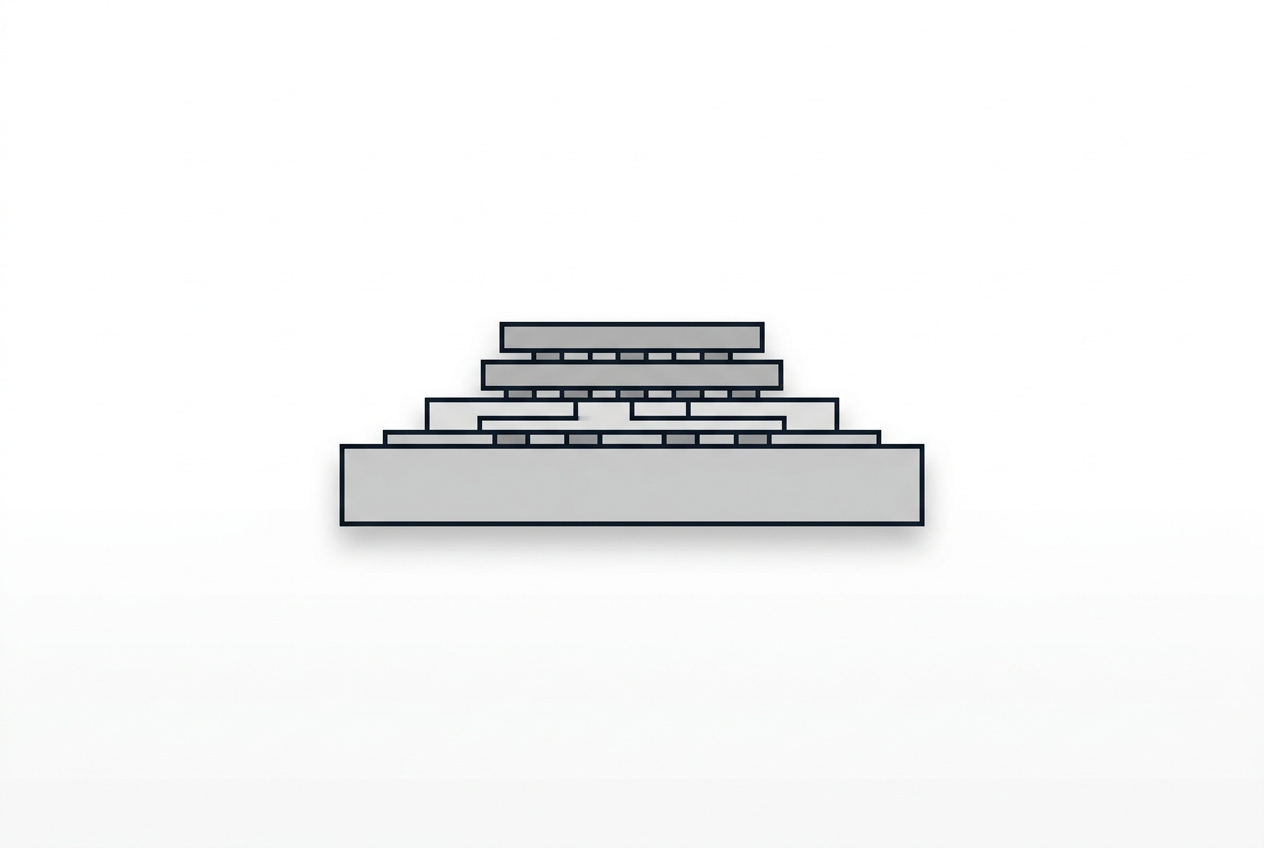
Every Blackwell die that leaves TSMC's Fab 21 near Phoenix travels roughly 7,000 miles to Taiwan to be diced, stacked, and mounted onto a silicon interposer via CoWoS-L, then travels onward through system assembly before any of it comes back to a U.S. data center.
That is the sentence Nvidia's "43 states, $500 billion over four years" blog post never writes.
TSMC's U.S. fabs currently send 100% of their chips to Taiwan for packaging — including the Blackwell wafers Phoenix now runs at volume on the custom 4NP node. The homegrown chip is homegrown right up until the wafer is finished, and not one step further.
The homegrown chip is homegrown right up until the wafer is finished, and not one step further.
Last week this column laid out the packaging chokepoint as an SK Hynix/TSMC integration lead that ran through 2027. This week the story hardened in the wrong direction: the freshest capital flows — Samsung's glass-core JV, Korean makers' first packaging fabs in China, UBS's aggressive new take on ASE — are all deepening Asian concentration, not reversing it.
Start with the money, because the money is the tell.
The CHIPS Act committed roughly $52 billion to front-end fabs and about $3 billion to advanced packaging through the NAPMP. That is less than six cents of every dollar going to the step that turns a working die into a chip you can solder onto a board.
The result is exactly what the incentives bought. Asia-Pacific holds roughly 74% of the OSAT market; North America sits near 15% by one count, and by the Global Electronics Association's tally the U.S. share of chip packaging is around 3%.
Front-end fabrication is capital-intensive, visible, and easy to photograph. Packaging is unglamorous, labor-heavy, and — until AI accelerators made it the binding constraint on who ships — treated as an afterthought that got farmed out to low-wage Asia decades ago.
"After the making of chips, packaging is the most important thing," said former Intel CEO Pat Gelsinger, who lobbied for the CHIPS Act. "And our packaging supply chains may be even more precarious."
Now watch where the 2026 capital is actually going.
UBS just lifted its ASE target to NT$835 — the street's highest — on a single premise: TSMC is expanding CoWoS faster than anyone modeled. The bank raised its estimate of TSMC's end-2027 CoWoS capacity from 150,000 to 180,000 wafers a month.
ASE's CoWoS-related revenue, on UBS's math, jumps from about $300 million this year to $2 billion by 2027. That is a surge — and every dollar of it lands in Taiwan.
In Korea, Samsung Electro-Mechanics signed a definitive agreement with Sumitomo's Dongwoo Fine-Chem to form a glass-core substrate JV named GlaSSEM, roughly KRW 480 billion, headquartered inside Dongwoo's Pyeongtaek plant, with production targeted for the second half of 2027.
Glass core is the next substrate frontier, and the deal wires it into Korean design capability plus Japanese materials chemistry — a Korea-Japan axis, not an American one.
And for the first time, Samsung and SK Hynix are reportedly planning semiconductor packaging fabs in Hunan, China, to add HBM-related capacity — their first packaging footprint in the province.
Read those three moves together and the pattern is unmistakable. The newest packaging investment on Earth is flowing into Taiwan, Korea, Japan, and China. None of it is flowing toward closing the American gap.
Here is the part that makes the gap unfixable this hardware generation: it is not merely a capacity gap. It is a physics-and-know-how gap that even the leaders haven't cleared.
Look at what just happened to Nvidia's Kyber rack. SemiAnalysis reports the Kyber NVL144 has slipped more than 12 months, to 2028, and the culprit isn't a fab — it's a printed circuit board.
The orthogonal backplane meant to carry the all-copper NVLink fabric between 144 Rubin Ultra packages is described as three 26-layer sections laminated into a single 78-layer stack, close to a square meter in area, with trace spacing at or below 25μm and impedance held within a 5% tolerance to keep 448 Gb/s signaling intact.
Nvidia also killed the NVL72x2 stopgap after its largest customers balked, leaving, per SemiAnalysis, "no proven solution to expand the scale-up world size for Rubin Ultra."
Sit with that. The most valuable hardware company in the world, working with the most advanced packaging house in the world, cannot yet manufacture a passive board to spec. If TSMC and Nvidia are stuck on the back end, the notion that a first-time American ecosystem catches up on the same timeline is fantasy.
Because the domestic answers all ship in 2028 at the earliest — the same window in which the leaders are still solving problems.
Amkor broke ground on its $7 billion Peoria, Arizona campus last October, with roughly $400 million in CHIPS funding and Apple and Nvidia as anchor customers. TSMC signed a 10-year packaging-and-test deal with Amkor on June 16. The first factory completes mid-2027; production begins early 2028.
TSMC's own Arizona packaging line — CoWoS and 3D-IC — won't come online before 2029, per its executives.
And the memory side finishes on the same clock: SK Hynix's $3.87 billion West Lafayette, Indiana packaging plant targets HBM4E and HBM5 mass production in the second half of 2028. So even the packaging-lead thread that runs through the memory story dead-ends at the same 2H28 wall on U.S. soil.
Now stack the calendars against the product roadmap.
The entire Blackwell family — and, on this evidence, the first Rubin generation — will complete its commercial lifecycle before any fully domestic finishing path exists. The first accelerator that can be fabbed, packaged, and fitted with U.S.-packaged memory without leaving the country is an HBM4E-era part arriving somewhere around 2028 to 2029.
Until then, every "American" AI chip is American until the wafer is done, then it's a Taiwanese finishing job.
The reason this can't be dollared away is that packaging is a different industrial discipline with its own equipment, substrate suppliers, specialty materials, and — most stubbornly — its own workforce, all of it clustered where the assembly volume already lives.
UCLA's Subramanian Iyer, a former IBM technologist who built one of the first interposers, watched the Trump administration effectively kill a $1.1 billion Arizona packaging R&D center last year. "We've ended up in a place where we are even more dependent on TSMC," he said. "They've thrown the baby out with the bathwater."
The engineers who know advanced packaging built their careers where the work was. Rebuilding that knowledge base takes years, not quarters — and a groundbreaking doesn't manufacture a technician.
So the reshoring debate has been fought at the wrong end of the line. America is genuinely winning the fab war: two companies now run leading-edge logic on two competing nodes in Arizona, a real achievement.
But winning the front end while the back end stays a Taiwan-Korea-Japan monopoly means the wafer victory is a partial one. The tier that actually decides who can ship AI compute — assembly, substrates, the materials-and-workforce ecosystem behind them — is controlled by exactly the actors reshoring was meant to route around.
And the freshest money is pouring into their geography, not ours. Homegrown Blackwell is, for this hardware generation, a marketing fiction with a 7,000-mile flight built into it.