Samsung Diverts Over Half Its 4nm Foundry to HBM4 Base Dies, Reshaping Logic Supply
Fifteen thousand wafers a month. That is reportedly how many of Samsung's 4nm SF4 wafers, out of a total of roughly 30,000, are now leaving the Pyeongtaek fab not as processors but as HBM4 base dies.
Put differently: up to 60% of Samsung's most advanced merchant logic capacity is being consumed by something that is not a chip in any sense a foundry customer would recognize. It is the floor of a memory stack.
Up to 60% of Samsung's most advanced merchant logic capacity is being consumed by something that is not a chip in any sense a foundry customer would recognize.
Two nodes ago, that sentence would have been a category error. A memory product drinking from the leading-edge logic well was not a supply-chain tension to worry about; it was a contradiction in terms. DRAM had its own fabs, its own processes, its own economics. Logic had SF4.
That wall is gone.
Last week in this space, the Korea story was about supply discipline on the memory lines — the big three deciding what to make and how long to withhold it. This week the same discipline has crossed into the foundry, and the object being rationed is no longer memory capacity. It is leading-edge logic wafers.
Start with the mechanism, because the allocation number only matters if the crossover is structural rather than opportunistic.
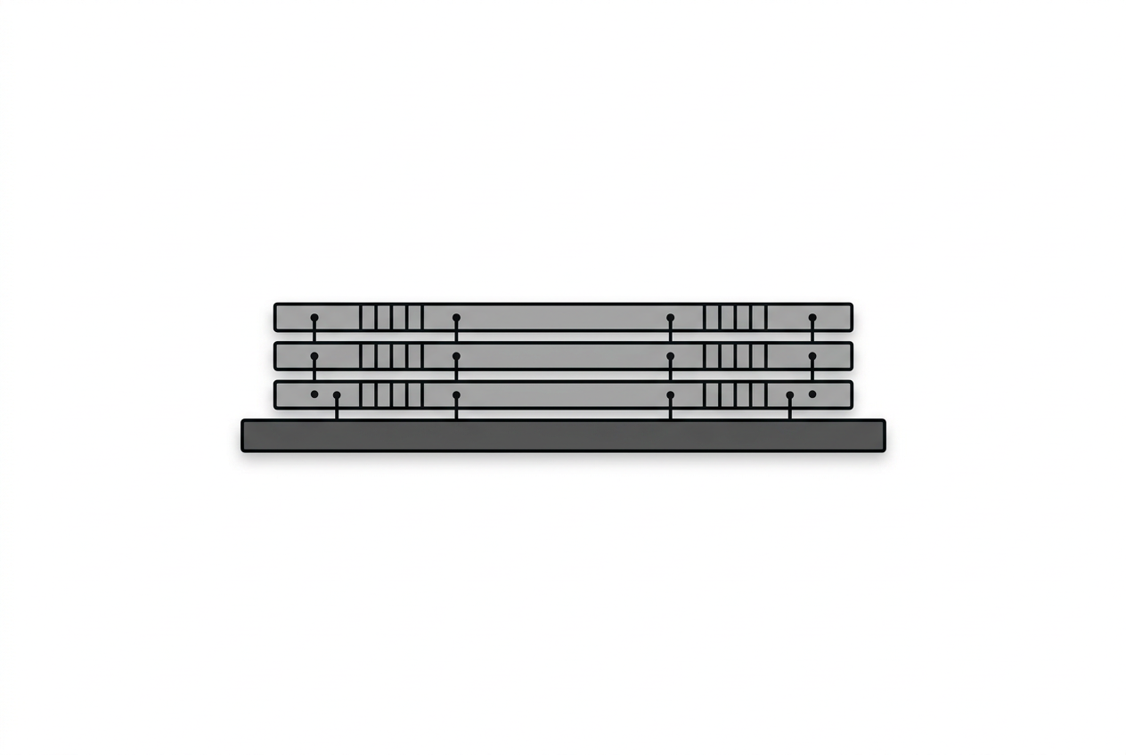
The base die sits beneath the vertically stacked DRAM core dies and manages data transfer between the memory and the system processor. Through HBM3E, it was largely a memory-division problem — base die and DRAM both handled inside the memory house.
HBM4 broke that arrangement. As data rates and pin speeds climbed, the base die became a performance bottleneck, and the only way to relieve it was to build it on a logic node.
Then the customers went further. Per Korean reporting relayed through TechPowerUp, buyers of HBM4 and the coming HBM4E are now asking for base dies stuffed with custom logic — memory controllers and PHYs pulled off the main compute chiplet and dropped onto the HBM base die itself.
That is the load-bearing detail. Once a controller or a PHY migrates onto the base die, the base die is no longer a passive interposer. It is a logic block with a floorplan, and it competes for the same SF4 slots an inference ASIC would use.
This is why the crossover does not reverse. Every generation of HBM raises the performance premium on the base die, which pushes more function onto it, which deepens its claim on leading-edge nodes. The pull scales with the roadmap, not with a single quarter's order book.
Samsung itself is telling investors as much. At a recent non-deal roadshow, the company framed the tightening link between its memory and foundry arms as the whole point — custom HBM4E and HBM5 designs paired with foundry-built base dies, sold as one product rather than two.
The Broadcom MOU reportedly signed in July, covering memory, foundry, and packaging together and pitched at more than $200 billion through 2030, is the same logic written as a customer relationship. Buy the memory, buy the base die, buy the wafers underneath it — all from one vendor.
Now the paradox, which is where this stops being a Samsung engineering story and becomes an industry-structure one.
Samsung is a foundry laggard. Its SF4 line was not full. According to Hankyung reporting via TrendForce, external inference-chip wins — Groq 3 among them, alongside other ASIC orders — had reportedly not been sufficient to fully utilize capacity.
An underfilled leading-edge fab is a bleeding wound for a foundry. Depreciation runs whether the wafers move or not, and the merchant customers who would fill it were choosing TSMC.
So Samsung filled the line with itself. Internal HBM4 orders ramped, and Pyeongtaek utilization reportedly pushed past 90%. The company that could not sell its 4nm capacity to the merchant market solved the problem by, in effect, becoming its own largest 4nm customer.
Read one way, that is a clever save — an idle asset converted into a captive input for a business with far better margins. Samsung had even reportedly planned to prioritize standard server DRAM over HBM4, then reversed course as HBM demand from Nvidia, AMD, and reportedly OpenAI hardened.
Read another way, it is the thing the industry should be watching, because of what it does to everyone who is not Samsung.
Leading-edge wafers are the most contested resource in the semiconductor economy. Until now, the claimants on that resource were all logic: CPUs, GPUs, phone SoCs, AI accelerators. They competed against each other, but they all answered to roughly the same economics — performance per wafer, sold as a processor.
HBM4 introduces a second kind of claimant, and it answers to memory economics instead.
That distinction is not cosmetic. When Samsung decides whether an SF4 wafer becomes a Groq base tape-out or an HBM4 base die, it is not comparing two logic products. It is comparing a foundry margin against an HBM margin — and HBM, in this cycle, wins that comparison decisively.
The base die is reportedly said to cost three to four times as much as a DRAM core die, and, per Alex Jenkins of WADSIH, HBM sells at a healthy margin while commodity DRAM was moving near cost. Stack that against merchant foundry pricing and the allocation decision writes itself.
Which means the merchant customer who wanted SF4 capacity is no longer bidding against other chip designers. He is bidding against Samsung's own memory division — a bidder with better unit economics and no reason to lose.
This is the quiet redrawing of the foundry-memory boundary. HBM has become a leading-edge logic consumer, and at Samsung it is a consumer that sits inside the house, with first call on the wafers.
The direction of travel is worse for the merchant pool, not better. An earlier ZDNet report, relayed by Wccftech, had Samsung reportedly weighing its 2nm technology for future HBM base dies, possibly repurposing a Giheung line, possibly reserved for Nvidia. If HBM's node appetite marches from 4nm to 2nm alongside the compute chips it feeds, the contention moves to the frontier rather than staying a generation behind it.
There is a defensible case that this is simply good asset utilization by a firm that could not otherwise fill its fab. That case is real. But it rests on Samsung being a laggard today — and the same integration that rescues an underused SF4 line becomes a lever the moment the line is full and demand keeps climbing.
SK hynix's chairman Chey Tae-won has reportedly already framed the wafer constraint as structural: "it is physically impossible to suddenly increase wafers in the short term. Securing more wafers takes at least four to five years." He was speaking about HBM, but the logic runs both directions. If HBM now eats logic wafers, the years-long lead time to add capacity becomes a years-long lead time before external logic customers get their slots back.
For now the shape is clear enough. A memory supercycle has found a way to consume leading-edge logic capacity directly, and Samsung is the first firm to prove it can be done at scale — half a fab, rerouted, in a single year.
What that scarcity costs buyers, and how the back-end packaging binds all of this together, is a separate question. Look elsewhere in this issue for those. The front-end story is simpler and, in its way, more unsettling: the well that logic drank from now has a second mouth on it, and that mouth answers to memory.