
"The Tesla-Samsung AI5 chip has reached tape-out. It is scheduled to be manufactured at the Taylor fab using our latest 2nm process."
That was James Kim, a principal engineer at Samsung Foundry, writing on LinkedIn. Not a press release. Not an earnings call. A career update, the kind of thing you post between congratulating a former colleague and endorsing someone's soldering skills.
And it moved an entire foundry's turnaround narrative.
Within days, Korean business press was framing Samsung's Taylor plant — reportedly a $37 billion facility that had sat waiting for anchor customers — as entering its "Taylor era." Industry watchers began predicting the foundry division would sharply narrow losses next year and return to quarterly profit. All from an engineer's honor to have collaborated with Tesla's teams in Palo Alto and Austin.
The gap between the disclosure vehicle and its market weight is the tell. When the most substantive confirmation of a chip program arrives as a LinkedIn humblebrag, you are looking at a story where the narrative is running well ahead of the silicon.
When the most substantive confirmation of a chip program arrives as a LinkedIn humblebrag, you are looking at a story where the narrative is running well ahead of the silicon.
So strip it down.
Start with what Tesla actually showed. In mid-April, Musk demonstrated the first AI5 sample: a relatively compact accelerator die — roughly half a reticle, by his own remarks — sitting alongside 12 SK hynix memory packages on an organic substrate.
Those memory packages appear to be standard GDDR6 or GDDR7 devices, labeled like conventional discrete DRAM. Twelve of them points to a 384-bit bus, which translates to somewhere between 768 GB/s and 1.536 TB/s of bandwidth.
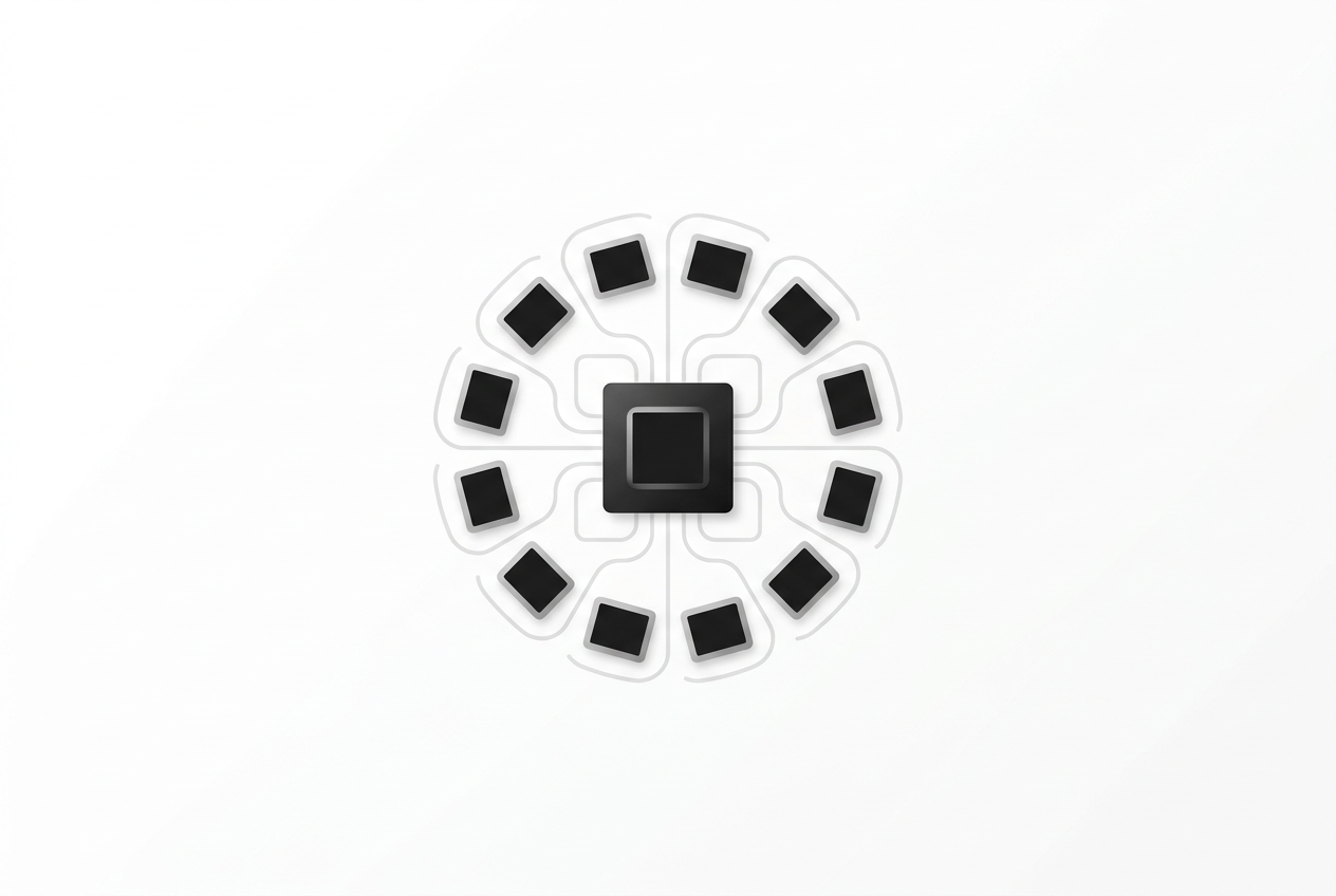
That is consumer-class memory. GDDR on an organic substrate is what you find on a graphics card, not the stacked HBM on silicon interposers that defines a datacenter training part. It is a design choice about cost and volume, not a bid for the memory-bandwidth frontier.
Now the performance claim. Musk has said AI5 delivers up to 40X improvement over its predecessor "in certain workloads." That is a comparison against Tesla's own AI4, in favorable conditions — a relative claim about generational progress, not a benchmark against anyone else's chip.
Apple's headline number gets the same treatment, and Apple is refreshingly explicit about it. Per Mark Gurman's reporting, the M7 Ultra's AI performance is described internally as approaching dedicated accelerators, with Nvidia's Blackwell as the reference point.
Gurman's own caveat: that is a relative claim, not a benchmark, drawn from an internal, multi-year roadmap where ship dates, configurations, and node targets can all move. The M7 Ultra isn't expected to ship until around 2028.
So neither "datacenter-class" flagship is competing with a merchant GPU on the merits it's implicitly invoking. Which raises the real question: if these aren't GPU-killers, what are they?
They are volume plays and vertical-integration hedges — and both are explicitly hostage to constraints their designers do not control.
Take Tesla first. Musk expects AI5 to be one of the most-produced chips ever, feeding cars, Optimus robots, and Tesla's own datacenters. That is the actual thesis: not peak performance, but performance-per-watt at fleet scale, driving down cost per inference across millions of units.
Volume, though, needs capacity. And capacity is why the dual-foundry move matters — not as a flex, but as insurance.
AI5 is being built at both TSMC and Samsung. The TSMC version taped out several months ahead of the Samsung one. That is not redundancy for its own sake; it is a hedge against single-source failure on a chip Tesla intends to make in unprecedented quantities.
The choice of Samsung's Taylor fab is where insurance becomes something stranger. Taylor is a testbed for Samsung's 2nm gate-all-around process — unproven at profitable yield. Tesla is effectively underwriting a US fab into existence, betting its highest-volume program on a yield curve that hasn't demonstrated it can climb.
If Samsung hits profitable yields in 2026, Tesla could, per Futurum, get a cost advantage over rivals stuck on more expensive single-source nodes. If it doesn't, Tesla has bought expensive complexity — two foundries, two process maturities, two yield profiles to manage on chips that may share design and software stacks.
Either way, Samsung is the accidental winner. Taylor's operation had been delayed for lack of a marquee customer. Tesla's AI5, plus a reportedly roughly 23 trillion won ($15.3 billion) AI6 deal running through 2033, gives the fab an anchor tenant and a validation story it can sell to every other American fabless firm — Nvidia, Qualcomm, AMD, and the AI labs like Anthropic that Samsung is courting.
That is the quiet structural consequence buried in an engineer's LinkedIn post: a customer's risk-management decision resurrecting a foundry's competitive position.
Apple's version of the hedge runs through the same bottleneck, from the other direction.
Apple has collapsed its roadmap around AI, skipping the M6 Pro, Max, and Ultra entirely — the first time it has ever skipped a full high-end tier — and taping out the M7 just six months after the M6. The organizing principle is no longer clock speed or GPU or thinness. It is neural performance.
The endpoint is a datacenter part: an M7-Ultra-based AI server, reportedly targeted around 2029, with up to 1.5TB of unified memory — roughly double the M5 Ultra — built to run Apple Intelligence inference on Apple's own silicon.
And here is Apple's own admission. That 1.5TB target is, per Gurman, contingent on the memory market. The ongoing DRAM shortage has made high-bandwidth memory scarce and expensive, and even Apple's datacenter roadmap is gated by supply it does not control.
Read those two admissions together — Tesla's GDDR-and-organic-substrate module, Apple's memory-contingent server — and the pattern is unmistakable.
Both companies are routing around merchant GPUs to escape the cost of buying Nvidia's stack. But the two things that make merchant silicon expensive in the first place — leading-edge fab capacity and a memory market controlled by a handful of suppliers — are the exact two things gating their alternatives.
Tesla's ambition is hostage to Samsung's unproven 2nm yield. Apple's is hostage to a DRAM market it doesn't own. Vertical integration doesn't dissolve those constraints; it just relocates them from a purchase order to a manufacturing bet.
The structural read, then, is narrower than the "datacenter-class" framing suggests. Consumer and auto players building captive accelerators do shrink demand at the top of the curve — but only for their own workloads, and only if the fabs and the memory cooperate.
They are not replacing Nvidia at the training frontier. They are carving out the inference volume they can serve themselves, at costs they can control, on hardware they can privacy-market — and even that is provisional.
Which brings us back to James Kim's LinkedIn post. It was, technically, just an honest update from an engineer proud of shipping something hard.
But it did the work a press release couldn't, because a press release would have invited scrutiny. The offhand register let the "Taylor era" narrative form before anyone asked the load-bearing question: whether Samsung's 2nm can actually yield, and whether the memory market will let any of these ambitions arrive on schedule.
That question is the whole story. The taped-out die is real. The capacity and the memory are not yet — and until they are, "datacenter-class" is scaffolding, not a building.