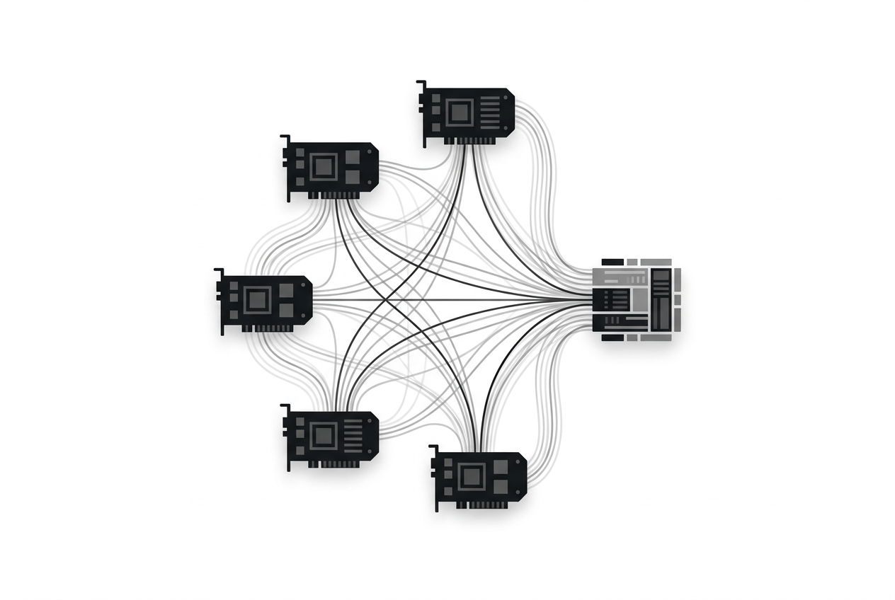
One hundred twenty-eight. That is the ceiling copper imposes — the maximum number of GPUs you can lash together electrically inside a single server before the wires themselves become the bottleneck.
Biren's answer, unveiled at the World Artificial Intelligence Conference in Shanghai, is 1,024. Eight times that limit, achieved not with a better chip but with light.
The company's next-generation supernode integrates optical engines directly onto its upcoming BR2xx boards using near-packaged optics, physically separating computing nodes from switching nodes so that fiber, not copper, carries the traffic between them.
"Optical interconnect has become an inevitable choice to break through this bottleneck," said Ding Yunfan, Biren's vice-president of AI framework architecture. Single-GPU performance, he argued, is no longer the game — the game is turning thousands of chips into one seamless machine.
Single-GPU performance is no longer the game — the game is turning thousands of chips into one seamless machine.
Last week in this space, the story was China's parallel compute stack built on Huawei silicon — domestic dies as a hedge against Nvidia. This week the workaround extends one link down the chain, from the chip to the thing that connects the chips.
And the tell is convergence. Biren was not alone on the WAIC floor. Huawei reportedly showed its Ascend 950 supernode — sixteen compute cabinets, 1,024 Ascend cards. Alibaba brought its Zhenwu M890 and Pangu supernode. ZTE displayed its OEX supernode. A domestically built 100,000-card cluster sat on the exhibition floor as a statement of intent.
Four rivals arrived at the same architecture in the same week. That is not a product cycle. That is an industry executing a shared adaptation and calling it a launch.
The engineering logic was articulated most cleanly not at WAIC but a year earlier, by Huawei founder Ren Zhengfei in a rare front-page People's Daily interview. He conceded China remains "one generation behind the United States" in conventional chips.
Then he laid out the escape route: close the gap by "compensating for physics with mathematics, for Moore's Law with non-Moore approaches, and for single-chip limitations with group computing."
Group computing. That phrase is the whole strategy. If you cannot etch a better transistor because you cannot buy the lithography, you stop competing on the transistor and compete on how many transistors you can make behave as one.
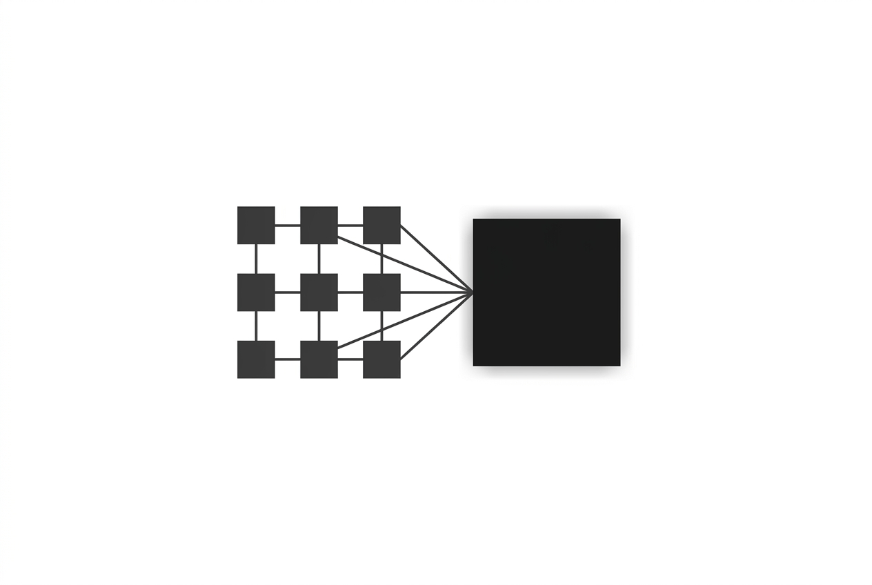
The supernode is that doctrine cast in fiber and steel. It converts constrained silicon — chips stuck at or behind 14nm — into competitive scale by lashing more of them together than copper ever allowed.
The second prong is the edge. Even as cloud players race toward trillion-parameter clusters, a cohort of Chinese AI chip startups is pivoting toward robots and smart hardware — running language models directly on devices.
The appeal there is that the physics stops mattering. On a robot or a phone, sub-14nm nodes are simply good enough; the frontier is irrelevant. So the edge is where Chinese silicon can compete on cost and integration rather than on process, sidestepping the sanctions entirely.
Between them, these two moves describe a coherent posture. At the frontier, aggregate around the chip ceiling with optics. At the edge, ignore the ceiling because you never approach it. Neither requires an EUV machine China cannot get.
Here is the catch, and it is structural.
The optical scale-out that makes the frontier strategy viable does not run on cleverness alone. It runs on materials and on a photonic supply chain that turns lab demonstrations into shippable product — and that is precisely where China remains dependent.
The Jamestown Foundation's own assessment is blunt: Chinese labs sit at or near the global frontier in photonic research benchmarks, but the United States and Taiwan still dominate the parts of the supply chain that convert those demonstrations into viable, scalable products. Leading a benchmark is not the same as owning a supply line.
Then there is helium. China produces roughly 1.6 percent of the world's supply, yet is reportedly restricting exports to protect its own — a gas critical to chipmaking and to cooling advanced EUV lithography systems.
Read that against the interconnect pivot and the irony sharpens. China is hoarding a material it barely produces, which tells you how tight the input constraints already are on the very manufacturing base the supernode strategy leans on.
So the workaround swaps one ceiling for another. It trades a chip ceiling China cannot lift — leading-edge lithography — for a materials-and-photonics ceiling it does not yet control either. The dependency does not disappear. It relocates.
And the third constraint is trust, which is being criminalized in real time.
On Monday, Taiwanese prosecutors handed down what the prosecutor's office described as the first indictment under the island's National Security Act aimed at leaking its most sensitive chip technology to China. The defendant, a former TSMC deputy manager surnamed Chen, allegedly copied 21 confidential documents, some covering technologies Taiwan designates as national core — a category that explicitly includes processes more advanced than 14nm.
The mechanism matters as much as the theft. Chen allegedly helped set up CSMAC, a semiconductor materials analysis company in China, and drafted a proposal called the "Blue Ocean Plan" to recruit Taiwanese chip workers into it.
That is state-directed talent poaching dressed as a business plan — and it is exactly the pipeline the group-computing strategy depends on, because systems-level engineering requires exactly the process and materials knowledge that lives in TSMC's people.
The transfer failed. TSMC's internal monitoring flagged the irregularities and recovered every copied document. But prosecutors called the case "highly significant" precisely because it is the first of its kind, and the National Security Act now makes that pipeline a felony rather than a gray-market job change.
The same wall is going up in the Netherlands. A Dutch government-funded study rated the country's semiconductor sector at "very high" risk of Chinese interference — above maritime, above aerospace — citing years of espionage against ASML and NXP.
ASML has already disclosed insider theft cases stretching back to 2015, including a former China-based employee who stole lithography data from an internal product-lifecycle system. The report now calls for tiered vetting of staff at sensitive sites and a public-private fund to rip out and replace high-risk foreign hardware.
The materials ceiling and the trust ceiling are the same ceiling viewed from two angles. ASML's optical systems reportedly depend on rare earths China restricted through 2025; China's photonic ambitions depend on knowledge and supply lines the West is now moving to fence off. Each side is tightening its grip on the input the other needs.
Which is the whole argument. The supernode is not vaporware — near-packaged optics linking 1,024 cards is real engineering, and it will hold at the edge, where good-enough silicon meets good-enough interconnect and sanctions have no purchase.
But at the frontier, the strategy is throttled by design. China has traded a problem it demonstrably cannot solve — buying EUV — for a set of problems it is betting it can: photonic supply-chain maturity, helium and rare-earth independence, and a talent pipeline that no longer requires importing indicted engineers.
The friction is the signal. Every indictment, every "very high" risk rating, every export restriction is a counterparty moving to close the exact door the workaround runs through.
Group computing lets China route around the chip. It does not let China route around the fact that the people it needs are now being arrested, and the materials it needs are now being counted.