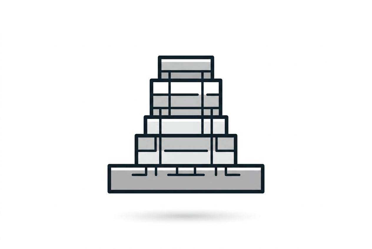
The most contested piece of intellectual property in the AI buildout right now is the shape of a die that does no computing and stores no data. On June 28, Samsung filed a patent covering the precise contour of the topmost layer in a high-bandwidth memory stack—the dummy die, a non-electrical lid whose only jobs are to make the package conform to a standard height and protect the cores beneath it. The patent specifies a three-tiered, stepped sidewall with discontinuous gradient shifts and upwardly convex curves, formed by deep-groove laser sawing rather than a mechanical blade, with micro-trenches pre-fabricated into the Non-Bonding Region to trap dicing debris. This is the level of obsession the industry has been driven to. At sixteen stacked layers, the thing most likely to kill your HBM stack is warpage at the top, and Samsung is now patenting the geometry of a protective cap to keep the whole tower from failing.
SK Hynix reportedly shipped 12-layer HBM4E samples to lead customers while Samsung was reportedly struggling on qualification. This week the story moves down one layer in the stack and one step further into the fab, because that is where the real governor on AI server output sits. Not the memory. The act of building and integrating it.
Start with the physics, because the physics is unforgiving. Moving an HBM stack from 8 layers to 12 layers triggers a 10-to-20 percentage-point drop in yield. Pushing toward 16 layers drives yields into the 40-to-60% range. That is not a manufacturing inconvenience; it is a wall. Each added die multiplies the surfaces that can delaminate, the interfaces that can micro-crack, and the cumulative warpage that throws off the through-silicon via bonds holding the structure together. Industry engineers describe top-die warpage in 12-layer-and-above configurations as a "make-or-break variable" for final yields. Samsung's odd little patent—the stepped lid, the laser grooves, the controlled 1-to-10-micrometer gap for heat dissipation—is best read as what serious yield work looks like at the frontier: not faster transistors, but desperate management of coefficient-of-thermal-expansion mismatch on a sixteen-story silicon building.
The bottleneck on AI accelerators is not silicon. It is the two stacked physical-assembly problems: yielding the tall stack, then interposing it at volume.
Now stack a second assembly problem on top of the first. Once you have a working HBM stack, you still have to mount it beside a GPU on a silicon interposer and integrate the whole thing—TSMC's CoWoS, chip-on-wafer-on-substrate. CoWoS production is reportedly running roughly 30% short of demand per analyst Handel Jones cited in The Indian Express, while other reports put demand at three times available supply; it is sold out through 2026 and into 2027. TSMC reportedly accounts for about 95% of all advanced packaging, per analyst Handel Jones. And the demand is brutally concentrated: Epoch AI estimates that the four largest AI chip designers—Nvidia, Google, AMD, and Amazon—consumed over 90% of global CoWoS capacity and HBM supply by value in 2025, while taking only about 12% of advanced logic die production.
Hold that asymmetry in your head, because it is the entire argument. Twelve percent of logic dies; over ninety percent of packaging and assembled memory. Logic fabrication is a soft constraint—most leading-node capacity serves other markets, so AI can grow its share by outbidding phones and laptops rather than waiting for new fabs. Packaging and HBM stacking cannot be outbid into existence. They require new facilities with multi-year lead times. The bottleneck on AI accelerators is not silicon. It is the two stacked physical-assembly problems: yielding the tall stack, then interposing it at volume.

You can see what this looks like from the buyer's side in Lenovo's order book. The company's AI server backlog has swelled to $21 billion in undelivered committed orders, growing even as it posts record revenue, because new orders arrive faster than hardware can ship. The flagship is the GB300 NVL72: 72 Blackwell Ultra GPUs and 36 Grace CPUs in a single liquid-cooled rack, each GPU reportedly carrying 279 gigabytes of HBM mounted on silicon interposers. Every server vendor tells the same story—Dell entered its most recent quarter with a $51.3 billion AI server backlog, HPE called its backlog the strongest it had ever seen. The binding constraint across all of them is assembled memory, the one link that cannot be substituted with parts from a dozen interchangeable vendors. A backlog is what it looks like when packaging capacity, not chip design, caps the industry.
This reframes who actually holds power—and it is not the framing Wall Street has settled on. The dominant narrative treats the three memory makers as the strategic layer: Samsung, SK Hynix, and Micron control roughly 95% of HBM, every wafer shifted to HBM displaces three wafers of standard DRAM, and that 3:1 ratio hands them durable pricing leverage as DDR5 prices spike. That pricing story is real. But it is downstream. Pricing power over a component is not the same as control over whether the component can be physically built and integrated at yield. Even the memory oligopoly's leverage is contingent on who can stack 16-high and who can interpose at volume.
And that capability is more concentrated than the memory business itself. Three firms split HBM. One firm—TSMC—reportedly does roughly 95% of advanced packaging, per analyst Handel Jones, and cannot keep up. The real chokepoint isn't an oligopoly; it's closer to a monopoly with a queue. Which is why the structural moves worth watching are the assembly moves. Samsung and SK Hynix are reportedly planning a semiconductor packaging fab in Hunan—their first such footprint there—explicitly to add capacity for HBM. SK Hynix and TSMC announced a collaboration to co-develop HBM4, optimizing the integration of memory stacks with logic at the foundry level, signaling a future where memory and packaging are designed in tandem rather than as separate purchase orders. U.S. chipmakers are pushing CoWoS-like work to OSATs such as Powertech and ASE through 2027. Nvidia is reportedly exploring Intel's EMIB. None of this is about who sells the most memory. All of it is about who can execute TSV stacking and interposer integration without the yield collapsing.
Which brings us to the "Micron is the next Nvidia" thesis, and why it is a category error that flatters the wrong layer. The argument runs that Micron, as the sole American HBM source, sits at a chokepoint equal parts geopolitical asset and technical moat—the company the AI industry "cannot build without." Parse that carefully. Being the only US-domiciled HBM producer is a procurement-policy asset: no US hyperscaler under an export-control regime wants a supply chain with zero domestic HBM sources, so Micron gets allocated demand by policy. That is valuable. It is not a manufacturing moat. The "next Nvidia" comparison even concedes the real bottleneck mid-argument—that HBM "requires advanced packaging, specifically a process called through-silicon via stacking, that only a handful of fabs in the world can execute at yield." Exactly. The scarcity lives in the stacking, not in being American. The durable veto belongs to whoever yields the 16-high tower and interposes it—and that, today, runs through Taiwan and a sold-out CoWoS line.
Nvidia's moat was CUDA plus a supply chain nobody else controlled. The memory makers' leverage is a wafer ratio. But the structural choke point underneath both is the one nobody is patenting press releases about: the physical integrity of a stacked package. When the most valuable intellectual property in the boom is the contour of a lid that does no work, you are looking at an industry whose true scoreboard is a yield curve—and whose strategic center has quietly moved from the people who make the memory to the few who can survive assembling it.